Tungsten Diselenide: From Discovery to Tomorrow’s Technology
Historical Development
Tungsten diselenide first caught the attention of materials scientists through the broad study of transition metal dichalcogenides in the early-to-mid 20th century. As semiconductor research picked up in the 1960s and 70s, the unique properties of layered compounds like tungsten diselenide started to attract more specialized interest. By the time thin-film technology and two-dimensional materials came into focus, tungsten diselenide was no longer just a curiosity on the lab shelf. The path from mineralogical oddity to research lab staple tracked along with major advances in solid-state physics, surface chemistry, and device engineering. Decades ago, few outside a tight circle of chemists could see its promise. Today, research papers, patents, and industrial demonstrations all draw on that original foundation, broadening tungsten diselenide’s reach outside pure academia and into high-impact fields such as optoelectronics and energy harvesting.
Product Overview
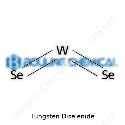
Tungsten diselenide, with the chemical formula WSe2, falls into the category of layered transition metal dichalcogenides. Each single crystal slice has a sandwiched structure: selenium atoms rest on both sides of a tungsten plane. Commercial labs usually supply it as a gray to black powder or pressed pellets, suited for further processing. The material finds regular evaluation as a field-effect transistor channel, photodetector, or as a catalyst for hydrogen evolution. Some suppliers favor selling high-purity, few-layer powder, while others focus on bulk crystals large enough for exfoliation. Researchers value strict controls on impurities, structural defects, and the presence of unreacted selenium or tungsten—factors that deeply influence electronic and catalytic properties.
Physical & Chemical Properties
WSe2 shows off a hexagonal, layered crystal structure, with each layer measuring just under 0.7 nanometers thick. Bulk crystals look metallic gray, with a sheen that reflects their tightly packed atomic layers. The density comes in at about 9.32 g/cm3, and the melting point rests just above 1200°C. Tungsten diselenide stays stable in air at room temperature, but can slowly oxidize when exposed to moisture and elevated temperatures. Its direct bandgap in monolayer form sits close to 1.6 eV, whereas the bandgap drops for multilayer and bulk samples. This band structure gives it promise for light-sensitive applications. Chemically, tungsten diselenide shows stability with acids but reacts in strong oxidizing environments, a trait that sets requirements for storage and handling.
Technical Specifications & Labeling
Standard specifications stress purity, particle size (usually in the micrometer range for powders), and layer count for few-layer samples. Laboratories order by purity levels—99.9% and up, with documentation including trace impurity analysis. Reputable suppliers print batch numbers, origin, production date, and handling guidelines on packaging labels, reflecting the growing attention to reproducibility and traceability in modern research. Some institutions now request full spectral analysis to confirm both crystallinity and absence of contamination from process residues, especially for use in high-precision or safety-critical devices.
Preparation Method
Most commercial or experimental batches rely on chemical vapor transport, direct reaction of tungsten and selenium powders at high temperature, or chemical vapor deposition for thin films. Chemical vapor transport employs iodine or bromine as the transport agent; a heated quartz tube keeps selenium and tungsten in circulation, growing large single crystals over a period of days. For powder, direct solid-state reaction provides the simplest synthesis, requiring a stoichiometric mixture sealed in an evacuated or inert atmosphere tube, then heated above 800°C. Chemical vapor deposition, on the other hand, involves volatilizing precursors and condensing WSe2 as thin films—critical for electronic applications where layer uniformity matters. Each method demands careful control of temperature, atmosphere, and precursor ratios, since even slight deviations can lead to selenium loss, unwanted phases, or subpar crystal quality.
Chemical Reactions & Modifications
Bulk WSe2 resists most chemical assaults, though exposure to strong oxidizers, such as hydrogen peroxide or concentrated nitric acid, introduces defects, etches the surface, or partially oxidizes the material. Researchers take advantage of this by selectively functionalizing surfaces, enabling device integration or catalytic performance tuning. Intercalation—forcing foreign atoms or molecules between the layers—finds use in battery research and for adjusting carrier concentration. Nanoscale modifications, such as edge functionalization or doping with suitable elements, have sparked interest for tuning photoluminescence and catalytic activity. Controlled plasma treatments can thin multilayer flakes down to monolayer sheets, yielding new phenomena absent in bulk crystals.
Synonyms & Product Names
Chemical catalogues and the scientific literature refer to tungsten diselenide under several names: diselenium tungsten, tungsten(IV) selenide, and the shorthand WSe2. High-tech vendors might brand it as “tungsten diselenide nanomaterial,” “high-purity WSe2 crystal,” or “monolayer WSe2 powder,” each label hinting at intended use or unique preparation. The CAS registry number 12067-46-8 acts as the unambiguous identifier, linking research, regulation, and production through a single code.
Safety & Operational Standards
Working with tungsten diselenide often takes place in fume hoods or glove boxes, especially during high-temperature synthesis, to protect against selenium vapor and fine dust. Inhalation of tungsten or selenium compounds brings respiratory hazards, urging the use of properly rated masks and localized extraction. Disposal practices require treating WSe2 waste as hazardous, respecting selenium’s environmental persistence. Laboratory SOPs stress spill containment, routine health monitoring for staff working with volatile selenium, and emergency procedures for accidental exposure. Institutions expect robust recordkeeping and batch traceability, both for quality control and hazard tracking.
Application Area
Tungsten diselenide serves as a building block in the next generation of transistors, photoresponsive sensors, and catalytic devices. Thin, flexible photodetectors draw on its stable bandgap and strong absorption in the visible spectrum. Solar energy researchers look toward WSe2 for its ability to split water molecules under sunlight, aiming for scalable hydrogen production. Layered WSe2 membranes, when engineered at the atomic scale, filter ions and molecules with far greater selectivity than many conventional materials. Some teams apply WSe2 as a lubricant additive, taking advantage of its layered structure to minimize friction. In the quantum technology sector, its direct bandgap and valley polarization properties keep it in focus for single-photon emitters and advanced optoelectronic circuits.
Research & Development
University and corporate R&D labs keep exploring tungsten diselenide’s electronic structure, stacking behavior, and interface chemistry. High-throughput synthesis and processing methods, aimed at scaling up monolayer film production, run alongside computational studies predicting new behaviors under strain, electric field, or chemical doping. Some teams grow heterostructures that pair WSe2 with other 2D materials—like graphene or MoS2—building entirely new device classes based on interface-controlled physics. Diagnostics, including STM, TEM, and ultrafast laser spectroscopy, keep pushing resolution limits to reveal stacking faults, defects, and grain boundaries. The strong interplay between experiment and simulation speeds progress, as machine learning models start predicting phase stability and synthesis outcomes from first principles.
Toxicity Research
With climbing research and manufacturing volumes, studies into tungsten diselenide’s toxicity attract serious attention. Early toxicological findings suggest that WSe2, as a bulk powder, releases little soluble selenium, but ultrafine particles or nanoplatelets may present distinct hazards from inhalation or accidental ingestion. Chronic exposure data remains limited—most animal or cell studies so far point to moderate cytotoxicity, especially at high doses or exposure durations, which aligns with known selenium compound risks. Regulatory agencies and research consortia now support long-term studies on accumulation in soil, water, and biological systems, mindful that nanomaterials rarely behave exactly like their bulk counterparts. Safety data sheets keep updating as more environmental and occupational exposure data appears, shaping handling rules for research and industry alike.
Future Prospects
As the world leans toward advanced photonics, energy storage, and catalysis, tungsten diselenide holds promise to drive step changes across several sectors. Large-area, monolayer films could one day anchor flexible electronics and wearable sensors, while tunable electronic structure may open doors to quantum device engineering. Hydrogen generation by solar-driven electrolyzers stands as a practical, near-term payoff, provided stability and cost hurdles fall. Further down the line, strong community interest in hybrid materials may see WSe2 stacked with organic molecules or embedded in polymer matrices, combining atomic precision with mechanical robustness. Investment in green synthesis techniques—especially solvent-free or low-waste methods—may help address outstanding toxicity and environmental footprint concerns. Every breakthrough publishes new questions: how to control defect levels, manage cost at scale, and move from demonstration to industry adoption. For students and scientists, working with tungsten diselenide today means joining a global quest to bend new materials toward cleaner, smarter technology.
Tungsten Diselenide in Electronics
Tungsten diselenide has grown popular among researchers and engineers building the next generation of electronics. Its layered structure lets it act as a semiconductor, but much thinner than traditional silicon. Folks making transistors can carve things down to the level of a few atoms, and they don’t lose the electrical control silicon transistors give. In the lab, tungsten diselenide helps create transistors that stay steady even as devices shrink.
Flexible electronics turn up everywhere these days, from rollable screens to sensors that stick to skin. Tungsten diselenide bends with the rest of the circuit without cracking or losing its function. This reliability springs from the way its atomic layers slip past each other instead of snapping. Makers of wearable tech lean on materials like this because they stand up to stretching and rolling far better than brittle traditional electronics.
Optoelectronic Devices and Solar Cells
Tungsten diselenide absorbs and emits light, and it’s good at it. Researchers working with lasers, LEDs, and light detectors reach for this compound when they want both sensitivity and control. Solar cells offer a good example. The stuff pulls in sunlight at certain wavelengths better than many old-school materials, which boosts efficiency. It doesn’t just absorb light; it converts it to electricity with fewer losses. The race to grab every electron from a sunbeam is tough, and tungsten diselenide gives solar cell designers better tools to win it.
Sensors You Can Trust
Chemical and biological sensors form another big area. One-atom-thick tungsten diselenide sheets act like the carbonation in a soft drink: they show a quick response when something interacts with them. They let scientists build sensors that pick up gases, poisons, and even biological signals at very low concentrations. Hospitals and environmental teams look for this responsiveness since it gives faster, more reliable warnings about what’s in the air or water.
Making Quantum Leap with Quantum Technology
Quantum communication and quantum computing call for materials that behave in reliable but surprising ways at tiny scales. Tungsten diselenide produces special excitons, which act a lot like messenger particles carrying unique information. Lab techs working on quantum light sources can harness those properties to build circuits beyond the limits of ordinary electronics. These advances open opportunities for safer communications and faster calculations, things experts say are coming soon to everything from banking to health care.
Medical and Imaging Uses
Medical teams and imaging researchers have started exploring tungsten diselenide as an ingredient for new types of diagnostic devices. Its thinness and electronic behavior help create ultra-sharp images and sensors that spot disease markers or physical changes in tissue. It withstands body fluids and sometimes resists cell buildup, which improves accuracy and cleanliness in devices meant to enter the body.
Challenges and Some Paths Forward
Despite promising applications, tungsten diselenide comes with problems. Making thin, defect-free films in large qualities tests manufacturers. Contaminants and cracks reduce performance, so better production methods remain high on the wish list. Recycling and safe disposal also matter since new technology brings new worries about environmental harm. More research—both in the lab and out in the field—can point the way to cleaner, more robust manufacturing.
The future for tungsten diselenide will depend on teamwork between researchers, industry, and government. Support for open data and new fabrication techniques can lower costs and boost reliability. If we keep learning from both successes and setbacks, this odd-sounding material could play an even bigger part in gear we use every day.
Grounded Experience with Tungsten Diselenide
Anyone who’s ever set foot in a research lab has brushed up against questions about material safety. Tungsten diselenide, a compound that gets a lot of attention in advanced electronics and nanotechnology circles, gets mixed reviews on safety. In every lab group I’ve worked with, tungsten compounds raise questions—often because most folks know little about their real risks beyond a quick glance at safety data sheets. From what I’ve seen, tungsten diselenide rarely triggers panic like lead, cadmium, or mercury. Still, responsible handling matters.
Understanding Its Hazards
Based on available toxicity data, tungsten diselenide (WSe2) does not show heavy-acute toxicity. The real sticking point comes from selenium. Too much selenium can trigger problems in the human body, with issues like nausea, headaches, and even neurological symptoms after serious exposure—think much higher than surface handling in a dry lab. Toxic effects rarely show up in routine settings, though. In a workbench environment, most risk relates to dust or powder inhalation, which is the case with practically all powdered nanomaterials. I remember a chemist telling a story of a minor powder spill that left everyone scrambling for dust masks. No one felt sick, but it changed how that team treats powdered solids, no matter the compound.
Touching tungsten diselenide does not compare with handling things like hydrofluoric acid or even some nickel salts. But there’s no immunity from risk, either. Chronic exposure in any poorly ventilated area, especially if workers get careless about gloves and goggles, could invite trouble. Skin contact seems less threatening, but powders sneak into cuts and under fingernails, providing a path for trace absorption. Over years, these micro-exposures can pile up. Caution always beats regret.
The Facts Backed by Science
Major toxicity studies, including those by the National Institutes of Health, highlight that tungsten metal and its stable compounds generally pass through the body with low uptake. On the selenium side, the body treats selenium dust very differently from elemental forms, sometimes leading to unpredictable bioaccumulation. Work done by research teams at the University of California pinpoints the particle size as a central factor: if tungsten diselenide reaches nanoparticle size, its “nano” status brings different hazards. Nano-structured powders behave in the lungs like silica and other fine particulates, possibly triggering inflammation or chronic lung problems after repeated exposure.
What Responsible Handling Looks Like
In the labs where I’ve handled tungsten diselenide, a few habits make all the difference. Use powder inside a fume hood, even for short tasks. Always wear gloves—nitrile makes a good default. Lab coats stop the dust from ending up on street clothes. Workers who wear safety goggles and simple disposable masks (rated for fine particulates) don’t worry much after clean-up. These practices stem from lessons written in accident logs: real safety depends on boring routines, not just emergency plans. After shifting to single-use weigh boats and disposable pipettes for nanomaterials, spills don’t wipe across surfaces, reducing that lingering worry about cross-contamination.
Looking Forward: Solutions and Respect for Materials
It doesn’t take an MD to see why curiosity about tungsten diselenide’s hazards runs high. More companies produce two-dimensional crystals like WSe2 every year. Training for workers and students can’t lag behind. Adding information about chronic exposure and best hygiene practices to onboarding sessions pays off more than any pricey monitoring gadget. Also, simple air quality testing before and after a project gives people confidence in their protection plans. Recognizing the small but real risks of selenium content means taking practical steps to reduce exposure, not shying away from the material entirely. With the right respect and a steady hand, most labs and even ambitious hobbyists can use tungsten diselenide without risking their health.
What Sets Tungsten Diselenide Apart?
Tungsten diselenide jumps off the page for anyone interested in new materials for electronics and optics. I remember first reading about it in a research summary, sandwiched between more common names like graphene and molybdenum disulfide. Tungsten diselenide stands out because of its unique mix of electrical and optical features. It stacks up as a transition metal dichalcogenide (TMD), and the personality it brings isn’t just surface-level—its two-dimensional layers hide a treasure trove of performance.
Electrical Properties with Real-World Impact
In my own work tinkering with photodetectors, I’ve seen how tricky it can be to get materials that both conduct efficiently and respond well to electrical control. Tungsten diselenide works as a semiconductor, with a direct bandgap measuring about 1.6 electronvolts in its atomically thin, monolayer form. That means it responds strongly to an electric field and can switch states with much less power and heat than traditional silicon. Bulk forms shift to an indirect bandgap, showing how tunable characteristics become with just a tweak in thickness.
Field-effect transistors made with tungsten diselenide have shown on/off current ratios far higher than many alternatives, meaning these switches don’t leak much current when off. This trait helps in designing smaller, faster processors and memory, critical when energy budgets push hardware design further each year. On top of the band structure, the strong spin-orbit coupling becomes a gate for next-generation quantum electronics. The physics here goes beyond theoretical interest—I talked to engineers working to leverage this spin splitting for new logic and storage devices that don’t lose information to heat as easily.
Optical Properties: Bright Prospects in a Thin Package
The direct bandgap isn’t just a winner for electronics. Optical experiments have shown tungsten diselenide absorbing and emitting light efficiently at visible wavelengths, peaking somewhere in the deep red. This sharp response makes it a natural pick for LEDs, low-power lasers, and solar cells that chase every last photon. I remember being in a university lab where researchers stacked monolayers onto silicon wafers with little more than tape and a microscope, and still turned out working optoelectronic devices.
Excitons—paired electrons and holes—roam longer and bind tightly in atomically thin tungsten diselenide, boosting light-matter interactions. Photodetectors built with it have blazingly fast response times, crucial for cameras, fiber-optic networks, or even light-based computation. This kind of strength in photon detection opens doors for medical diagnostics, environmental sensors, and telecommunications.
Pushing through the Challenges
Challenges pop up all over, though. Growing tungsten diselenide as a perfect sheet, free from defects or grain boundaries, continues to slow down commercial scaling. Chemical vapor deposition offers a path, but making large, uniform samples that don’t lose performance remains tough. Contact resistance between tungsten diselenide and connecting metals also saps efficiency, especially for high-speed circuits.
Researchers across Asia, Europe, and the US are jumping in to solve these problems—by doping the tungsten diselenide, layering it with other 2D materials, or experimenting with new electrode designs. I’ve seen startup labs reach out for cross-disciplinary collaboration, blending chemistry, physics, and mechanical know-how in pursuit of that next leap.
Where Tungsten Diselenide Heads Next
From quantum computing to ultra-sensitive imaging, tungsten diselenide offers plenty of incentive to push further. It doesn’t get the same splash as graphene, but it brings its own set of tools and quirks for building smaller, smarter, faster devices. In the hands of scientists willing to get their hands dirty with the stubbornness of materials science, it stands as more than just another lab curiosity. The electrical and optical properties create actual hope for tackling the data and energy demands that aren’t slowing down.
Navigating the Chemistry Lab Realities
Tungsten diselenide isn’t something you come across too often outside a research lab. Folks interested in new materials, especially those who pay attention to two-dimensional (2D) substances, know it for its use in electronics and photonics. Tungsten diselenide, or WSe2, has a crystal structure that lets it behave a bit like graphene—except it comes with a built-in band gap, so scientists look to use it in transistors and sensors. Every application, though, starts at the point of synthesis, and that’s where the story gets interesting.
Mixing Materials: From Powder to Crystal
Synthetic chemists like to get their hands dirty, and for WSe2, they usually reach for tungsten metal and selenium powder. The main method still relies on direct chemical reaction—place the powders in a sealed tube, pump the air out, and let things heat up. Temperatures reach close to 700 to 1000 degrees Celsius, high enough that everything melts and atoms from both powders combine to form WSe2. This isn’t something you try in your garage. The set-up demands steady hands and a keen eye. Leak-proof tubes, a steady flow of inert gas like argon, and good heat control matter a lot because you want pure WSe2 without leftover tungsten or selenium.
People shouldn’t underestimate how tricky it gets to produce high-quality crystals. In my own undergraduate lab work, even simple metal chalcogenides gave us headaches—small impurity changes led to big changes in results. In real labs, scientists grind, purify, and test powders repeatedly to find the right mix so the end product behaves as expected.
Growing Single Layers: Chemical Vapor Deposition (CVD)
Those who build tiny electronics usually prefer their tungsten diselenide in atom-thick layers. That’s where chemical vapor deposition comes in. In this technique, scientists load a furnace with tungsten trioxide powder and selenium, placing a smooth substrate like silicon nearby. Temperatures rise, the powders turn to vapor, and the vapor settles as a thin WSe2 sheet on the substrate. This method offers more control over thickness—a crucial edge for electronic and photonic uses. Controlled environment, timing, and temperature all help produce a layer just a few atoms thick. Each variable tweaks the performance of the final film.
While CVD remains the most common for 2D layers, it’s far from perfect. Thin-film makers keep pushing for cleaner, repeatable processes because defects in these ultra-thin films degrade device performance. A little stray moisture or temperature fluctuation can ruin a whole batch. Factories and university labs can both struggle with these sensitive steps.
Potential Solutions to Ongoing Challenges
Batch consistency and purity still give researchers plenty of grief. Reaching new levels of quality might come from smarter automation and better in-line monitoring during growth. More universities and companies are now sharing detailed experimental data, which feeds into machine learning models that predict and fix common synthesis issues. Over the past five years, more labs have begun using real-time sensors to detect impurities as they arise, allowing small course corrections instead of scrapping entire runs.
A move toward greener chemistry could also matter. Once you’ve spent a few years handling toxic selenium vapor, you start wishing for safer alternatives. Research into using solution-based methods, or milder precursors, has been growing. These aim to lower the health risks and the environmental impact of mass production, though scaling up remains tough.
Looking at the bigger picture, getting tungsten diselenide out of the pages of academic journals and into commercial products depends on cleaner, more reliable, and cost-effective synthesis. Every layer, every crystal, and every powder sample tells a story of trial, error, and hard-earned progress.
A Close Look at Commercial Offerings
Anyone looking to buy tungsten diselenide these days has probably noticed a few things: high tech buyers want purity, and labs need the right form. It’s easy to understand why. During my time consulting for a university nanomaterials project, I saw how even small impurities could throw off results or lead to expensive failures. Most factories now supply tungsten diselenide with more than 99.9% purity. In published research, you’ll often see claims of 99.99% or higher, sometimes marked as 3N or 4N. This isn’t just a marketing push—these purity levels help ensure repeatable results, especially in optoelectronics, energy storage, and chemical sensing.
Why the Details Matter
Experience shows that a small amount of nickel or iron can cause all sorts of problems, like weird shifts in electrical properties, or unpredictable layer growth. These issues tend to show up fast under the scrutiny of modern spectroscopy tools. For commercial labs and manufacturers, it just makes sense to pay for the highest available grade. The global standard now leans toward 99.99% purity for applications like field-effect transistors or photodetectors.
Popular Forms in the Marketplace
I remember ordering for a research group that constantly debated between powders and crystals. Most commercially available tungsten diselenide arrives as a gray or dark powder, finely milled (<10 microns), which is helpful when mixing with solvents or spreading into thin films. The powder works well for those running solution processes or creating printable electronics.
For groups focused on advanced electronics or fundamental physics, bulk crystals are much more desirable. Vendors usually provide small platelets or chunks, sometimes grown via chemical vapor transport (CVT). These crystals often look like shiny silvery flakes. Once in hand, they can be sliced down to thin layers, sometimes only a few atoms thick, with a sharp blade or even tapes. These monolayers reveal properties that make them so interesting to technology companies: flexibility, direct bandgaps, and easy integration with silicon. Powder suits big batch processes and composites, while the crystal form sets the stage for breakthroughs in two-dimensional material science.
Quality Control and Market Challenges
The biggest problem buyers face today isn’t just getting high purity, but making sure that purity matches what’s on the label. During my stint in quality assurance, audit trails often uncovered batches with traces of unlisted elements. Some producers struggle to keep oxygen and moisture away, and tungsten diselenide can react at high temperatures to form oxides. These side reactions impact electrical performance. Procurement experts now place more trust in certifications backed by third-party testing, especially for large contracts.
What Can Improve the Scene?
Suppliers could tighten up batch-level documentation. Routine spectroscopic analysis—XPS, ICP-MS—should become standard, not a premium service. Scientists working at the cutting edge need open channels to communicate with suppliers and quickly flag irregularities. If companies leading high-purity production collaborate with universities, sharing findings on best storage practices and contamination risks, everyone will benefit. Better labeling and more transparent sourcing would keep the market honest and reliable.
From lab bench to production line, the story behind tungsten diselenide’s form and purity matters as much as the material itself. Staying vigilant helps projects launch on time, with fewer technical surprises along the way.