Copper(I) Selenide: History, Properties, Applications, and Road Ahead
Historical Development
Copper(I) selenide caught the curiosity of scientists as early as the 19th century, blending the intrigue of chalcogen chemistry with the utility of copper compounds. Back in those early labs, researchers looked for ways to combine copper with selenium, taking cues from its more famous sibling, copper(I) sulfide. Results published through the decades led to better preparation routes, improved purity, and deeper dives into its electronic structure. Gradually, this compound attracted attention from both industrial chemists and physicists who saw potential in its unusual combination of metallic and semiconducting traits. The evolution didn’t come from thin air. Discovery often started with basic, sometimes crude, methods of mixing copper salts and selenium sources at controlled temperatures, and later advanced with better control over stoichiometry and purity. Over the years, folk in both the West and East contributed to refining methods, leading to a more reliable understanding of how to prepare and apply this golden-brown solid.
Product Overview
Copper(I) selenide doesn’t draw crowds like gold or silicon, but its role is hard to overlook wherever thin film technology, photovoltaic research, and thermoelectric applications run deep. Commonly sold as a dark, powdery solid, the compound lands in labs labeled Cu2Se. Producers typically offer various degrees of purity, with research-grade samples reaching 99.99% or higher, since small impurities sharply affect its properties. Researchers prize it for good electrical conductivity and its ability to shift from semiconducting to metallic character with changes in composition, temperature, or pressure. This chameleon-like switch contributes to its value, especially where energy or electronics technology meets experimentation.
Physical & Chemical Properties
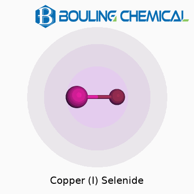
Copper(I) selenide stands out as a member of the selenide family with a unique cubic or orthorhombic crystal structure, depending on how conditions favor its formation. Visually, expect a black to dark brown powder, though in pellet or crystalline form, it can have more metallic luster. This compound carries a density near 6.7 g/cm3 and a melting point close to 1,100°C. In air, it resists oxidation better than some cousins like copper(I) sulfide, but long exposure at high temperature does trigger surface changes. Solubility in water remains negligible, but it reacts with dilute acids, generating hydrogen selenide—a gas that’s as toxic as it is rare. Electrical properties can shift from semiconductor to near-metal, based on composition and external stress. In my experience reading studies on thermoelectric materials, this flexibility keeps interest high among engineers and material scientists.
Technical Specifications & Labeling
Commercial offerings of copper(I) selenide often arrive with detailed labeling. Purity levels wind up listed above all else, since trace iron, nickel, or sulfur introduce unwanted interference in sensitive studies. Particle size distribution finds mention, especially for those using it to make thin films or nano composites. Moisture content, residual oxygen, and “free” selenium or copper also feature on spec sheets, recognizing their role in shifting conductivity or catalytic activity. Labels must register hazards since selenium compounds sit far from the “safe” end of the chemical spectrum. For researchers, clear handling and storage requirements save costly mistakes or accidents. I recall an incident where overlooked labeling on an impure batch confused a series of electrochemical measurements for weeks.
Preparation Method
Making copper(I) selenide in the laboratory usually starts with a reaction between elemental copper and selenium powder, heated in an inert atmosphere like nitrogen or argon. Folks rely on tube furnaces to reach 700–1,100°C, soaking the mixture to ensure complete reaction. The resulting mass cools under argon to avoid oxidation. A different route taps into copper(I) salts like copper(I) chloride, reacting them with selenide ions in aqueous solution, though this brings more impurities and less control over stoichiometry. Industry-scale prep demands strict control over atmosphere, time, and temperature, since stoichiometric deviations change both color and properties, shifting electrical behavior wildly. Researchers seeking nano-sized products use solvothermal or hydrothermal methods, tweaking solvents, surfactants, and pressure. The path you pick shapes the product’s eventual use, so process understanding grows ever more crucial as the applications web widens.
Chemical Reactions & Modifications
Copper(I) selenide gets involved in more reactions than many would guess from a basic chemical handbook. Subject it to strong acids and hydrogen selenide leaps out—a fast reminder to handle this stuff with care. Heating in excess selenium leads to copper(II) selenide or mixed phases, notably shifting electrical and optical behavior. Grind it with sulfur or expose it to sulfidation, and you open the door to tailored copper-containing semiconductors. Hold it in reducing or oxidizing atmospheres, and its structure transforms, granting new band gaps or improved conductivity. Surface modifications, such as doping with silver or alloying with tellurium, catch the eyes of nanotechnology teams aiming to fine-tune thermoelectric or optoelectronic properties. Over time, these modifications let copper(I) selenide punch above its weight in both classical and next-gen tech.
Synonyms & Product Names
Cuprous selenide and copper selenide pop up most often in scientific papers, though “dicopper selenide” sometimes surfaces, especially in older literature. On international markets, you’ll also find designations like Copper(I) Selenide, Cu2Se, “Selenocuprite,” and manufacturer-specific trade names. While these names mostly refer to the same composition, variant labeling or misidentified oxidation states can trip up the unwary; anyone working with product catalogs or search engines can vouch for that confusion at some point. Consistent naming supports clear communication, especially when ordering from suppliers across borders.
Safety & Operational Standards
Copper(I) selenide offers rewards with risks. Selenium compounds pack serious toxicity, and hydrogen selenide gas produced under acid attack ranks as one of chemistry’s more dangerous substances. Labs keep copper(I) selenide behind fume hoods, with personal protective equipment a strict requirement—gloves and eye protection included. I’ve seen the consequences of ignoring these standards, from headaches and nausea in minor incidents to outright laboratory evacuations. Handling protocols require secure storage, away from acids and bases, and careful cleanup of spills. Waste stream handling for copper and selenium calls for designated hazardous waste paths, monitored by environmental officers. Training and strict oversight limit accidents and protect both staff and the building.
Application Area
The magic of copper(I) selenide lies in its applications across energy technologies and electronics. Thin film photovoltaic cells rely on it as part of absorber layers, where it helps snatch photons from sunlight and convert them with decent efficiency. Thermoelectric devices, built to harvest waste heat in cars or factories, look to copper(I) selenide for its temperature-dependent conductivity, which flips as conditions change. Superionic conductivity—a quirky property in high-temperature copper(I) selenide—makes it useful for solid-state batteries and ionic conductors. In catalysis, researchers test it for organic coupling reactions and gas phase transformations, always on the hunt for new, cost-effective catalysts. Beyond energy, it appears in some infrared detectors, sensors, and experimental electronic components. Practical products still lag behind laboratory promise, yet each new research paper finds a new angle.
Research & Development
Scientific journals brim with studies exploring copper(I) selenide’s crystal structure, electrical transport, and defect chemistry. These lines of inquiry aim to unlock even better thermoelectric behavior or more robust photovoltaic cells. Nanostructuring takes center stage—scientists shape copper(I) selenide into nano rods, wires, or films, squeezing out new magnetic or optical effects. Industry partners push for scalable, cost-efficient preparation, aware that purity and stability dictate whether copper(I) selenide leaves the lab for factory floors. I’ve watched research at the intersection of energy and materials science grow more collaborative, since reliable data and cross-lab comparisons guide faster progress. Still, many questions about defect control, phase stability, and long-term degradation stay on the table, urging deeper investment from both public and private sectors.
Toxicity Research
Toxicology studies remind anyone working with copper(I) selenide to stay alert. Selenium intake at high levels brings on gastrointestinal distress, liver damage, neurological symptoms, and, at worst, death. Animal studies show that even trace exposure over time can bioaccumulate; the compound’s insolubility spares acute effects but doesn’t eliminate risk. Workplace exposure standards limit airborne particulate levels to parts per million. Chronic exposure warrants regular medical checks, and facilities need to monitor both air and surfaces for contamination. I’ve read case reports where missed safety steps led to lasting health problems, reinforcing the necessity for real-time monitoring, staff education, and robust protective policies.
Future Prospects
New uses for copper(I) selenide hinge on progress in nanotechnology, electronics, and power conversion. As demand surges for wearable tech, microgrids, and off-grid solar solutions, researchers see copper(I) selenide-based devices as potential game-changers, thanks to their ability to merge flexibility with good efficiency. Ongoing efforts seek to tame its toxicity and stabilize it in real-world conditions, easing transfer from research bench to market. Forward-thinking companies invest in novel synthesis methods that lessen environmental impact and improve cost per unit. Success will depend on both smarter preparation and deeper understanding of the compound’s behavior over years, not just in the short window of a single experiment. Efforts to recycle selenium and copper also help balance environmental cost with performance push, paving the way for copper(I) selenide to show up far beyond today’s limited markets.
Digging Into the Use Cases
Copper (I) selenide brings a spark of innovation to the table most folks don’t see coming. Once you start reading up on semiconductors and materials that power the electronics around us, this compound pops up in more places than expected. The real kicker is not just that it exists, but that people use it with a clear purpose in mind—to solve genuine challenges in energy, optics, and sensors.
Solar Cells and Renewable Energy
One big push behind research into copper (I) selenide comes from the green revolution. Solar panels used to be clunky and costly, mostly silicon wafers that demanded energy-hungry manufacturing. Now, scientists turn to materials like copper (I) selenide to build thin film photovoltaic cells. These films collect sunlight and shift it to electricity, all while using less raw material. That helps cut both the bill and the carbon footprint. Studies from journals like Solar Energy Materials and Solar Cells highlight how pairing copper (I) selenide with other compounds improves efficiency. The payoff shows up in better output for every dollar spent, which matters to both the environment and folks footing the bill for clean energy.
Electronics and Sensors
Current flows behave in strange ways at the nanoscale, which is where copper (I) selenide steps in again. Engineers turn to it for building sensors and electronics that live on the edge of what’s possible. The secret sits in its ability to shuttle charge with ease, making it a good pick for thermoelectric sensors. Right now, research labs push the limits for smaller, more accurate temperature and gas sensors using this copper-based material. Its flexibility also gives wearable device makers more room for ideas that go beyond what rigid circuits can offer.
Advanced Glasses and Coatings
Walk into a high-end optics lab, and chances are you’ll run into glass treated with compounds like copper (I) selenide. The draw here comes down to infrared light. Military and industrial teams need goggles and camera lenses that see in the dark or through smoke, and this selenide compound makes it happen. By changing the way light passes through glass, manufacturers cut out glare and sharpen images, which means safer flights, better medical scans, and smarter surveillance systems. Research from the Journal of Non-Crystalline Solids backs up these advances, showing the boost in performance in real-world applications.
Challenges and The Way Forward
The rise of copper (I) selenide brings new questions, not just solutions. Selenium itself demands respect; trace amounts support life but too much tips the balance toward toxicity. Safe handling, responsible sourcing, and proper disposal matter. Companies and universities that build with this compound need strong safety protocols and transparent reporting to protect workers and the environment. Regulatory agencies set exposure limits for selenium, so researchers check inventories and waste streams to prevent accidents. It pays to stay informed and collaborate across disciplines here.
Big Picture: Connecting Science to Daily Life
Innovation never happens in a vacuum. Seeing copper (I) selenide at work in fields like solar energy, sensor tech, and optics reminds me how chemistry can break down barriers, opening up new choices for energy, safety, and exploration. The lesson here is simple: everyday progress starts with materials that work quietly, shaping the world from behind the scenes. It takes curiosity, careful hands, and shared responsibility to turn these breakthroughs into daily essentials.
Getting Familiar With Cu2Se
Copper (I) selenide goes by the formula Cu2Se. Seeing those subscripts brings back memories of high school chemistry – counting atoms, learning about ions, trying to balance equations without losing your mind. Cu2Se means you get two copper atoms paired with one selenium atom. Unlike the copper you might find in an old penny, this compound carries different properties, landing it a spot in labs and research papers instead of in your pocket.
Where Cu2Se Fits In
Cu2Se shows up in solar cell development, battery improvements, and advanced electronics. The interest isn’t just academic, either. Light hits this compound and creates a response that can be harnessed – think of better ways to store energy or capture sunlight more efficiently. The appeal comes from its semiconducting behavior, plus the fact that copper and selenium combine to give a unique set of properties.
During some early experiments in college, I worked with compounds like these in a lab project aimed at forming new semiconductor materials. Mixing up copper and selenium, heating them carefully, and hoping the ratios turn out right, you start to appreciate the hands-on challenge behind getting that Cu2Se to form cleanly without extra unwanted compounds. This formula isn’t some trivia fact – it sets the stage for real, sometimes painstaking work with potential payoffs for clean energy and better tech.
Why Details Matter
Anyone trying to work with copper (I) selenide needs the formula to avoid confusion with other copper selenides. Missing a subscript or not realizing whether copper’s sitting in a +1 or +2 oxidation state can lead down the wrong path. You might think you’re getting CuSe or CuSe2, but Cu2Se brings unique characteristics, especially when tuning materials for electronics or investigating ways to make solar technology more affordable.
Looking through scientific articles or patent filings, Cu2Se pops up as a contender for thermoelectric materials. Scientists like it for how it handles heat and electricity – crucial in designing devices that need both. Getting the chemistry right makes sure that research can move from the bench to usable products. Muddling up formulas wastes time and resources, and in large-scale production, mistakes can turn costly fast.
Challenges and Real-World Solutions
A common challenge with Cu2Se comes from controlling purity and getting its structure just right. Too much copper, or a selenium deficiency, changes how the material behaves. Labs use various synthesis methods, like melt reactions or chemical vapor transport, to get the right ratio and structure. Each production step gets checked for quality to make sure the final product really matches the formula written down.
Safer handling of selenium, which can pose risks if mismanaged, matters just as much. Facilities and workers take special care to use protective gear and containment. These steps protect health and keep operations within safety regulations, something everyone can appreciate whether they’re in a classroom or a cutting-edge research lab.
Looking Forward
The future for Cu2Se depends on how well scientists can manipulate its properties for new technologies. As more teams push for breakthroughs in energy and electronics, having the right formula isn’t just academic—it’s the key to progress. Each chunk of copper (I) selenide, formed with the simple formula Cu2Se, holds the hope of cheaper solar cells or more durable batteries. Precise formulas shape real-world innovation, showing chemistry is as practical as it is fascinating.
Beyond the Test Tube: What’s Really in Play
Copper (I) selenide doesn't usually show up on a household shopping list, but it does pop up in labs and some high-tech industries. Those small dark crystals—Cu2Se, for the curious—fit into all sorts of applications, from semiconductors to solar tech. Yet the real question isn’t just how well it conducts electricity. It’s what happens if you actually have to work with it.
Looking at Toxicity and Real Risks
Nobody should brush off a material just because it’s tricky to pronounce. The first flag actually comes from selenium’s side. Selenium is a trace element, so the body needs a little bit. Too much isn't good news. It heads into toxic territory. That’s true for plants, animals, people. Now put selenium in the form of copper (I) selenide, and you compound it with copper’s own issues—copper dust can hurt your lungs, and chronic overexposure does damage to the liver and kidneys.
A few grams tossed around in open air might not cause instant horror, but even basic chemistry shows selenides can decompose into hydrogen selenide gas under acid or heat. That one—H2Se—smells like rotten horseradish and can be as deadly as hydrogen cyanide. In my university lab years, nobody broke open a bottle of copper (I) selenide without gloves, a mask, and sharp respect for the fume hood. The rule: treat every part of the process as a chance for bad news, not just the powder but any byproducts coming from spills or experimental mistakes.
Environmental Side: Not Just a Workroom Problem
Factories and mines that deal with copper or selenium waste have a real headache. Accidental releases—whether it’s dust, waste water, or ash—move selenide compounds into the ground or rivers. The wildlife story isn’t cheerful. Selenium builds up in fish, birds get sick, eggs don’t get laid, and populations drop. Traditional water filtration barely touches metallic selenides, so dumping waste just hands off the problem to the next community downstream.
Taking Responsibility with Copper (I) Selenide
A company that treats copper (I) selenide as “just another lab chemical” is asking for trouble. The smarter approach looks to minimizing dust, keeping tight lids on storage, and real training for everyone from lab techs to janitors. I once saw a chemist handle this compound without realizing a minor acid spill could trigger selenide gas. The point gets hammered home—don’t get complacent.
Reliable data matters here. The Occupational Safety and Health Administration (OSHA) and National Institute for Occupational Safety and Health (NIOSH) both list selenium compounds as a priority, setting workplace limits for airborne exposure. Studies by the International Agency for Research on Cancer (IARC) continue to probe whether chronic exposure affects cancer risk. Meanwhile, the U.S. Environmental Protection Agency (EPA) keeps tabs on selenium in drinking water, alert to the possibility of accidental selenide pollution.
Better Practices, Safer Outcomes
Smart labs and factories don’t just rely on paperwork or warning labels. They bring in local exhaust systems, double-check chemical storage, and teach everyone the signs of selenium poisoning—fatigue, digestive distress, nail or hair changes. For spills, immediate cleanup becomes routine, not a rare emergency. Used packaging and waste get tracked, labeled, and shipped off for proper disposal rather than junked in local trash.
Anyone dealing day to day with copper (I) selenide gets reminded quickly: this isn’t just a number on a periodic table. It’s a real risk, and it deserves respect.
Understanding Copper(I) Selenide
Copper(I) selenide, or Cu2Se, doesn’t come up at backyard barbecues, but it matters a lot in the right lab or factory. With its semiconductor properties, research teams use it in photovoltaics, sensors, and thermoelectrics. Still, talking chemistry often skips the basics: keeping it safe, pure, and reliable for the next project. Every bottle has a price tag, and mishandling turns valuable material into trash.
The Realities of Storing Reactive Materials
Those who have spent time in a university materials lab or an industry stockroom know supplies pile up fast and mistakes haunt you later. Cu2Se isn’t as famous as sodium or potassium, but it puts up a fight against air and moisture. Left out, the air attacks it, and humid conditions worsen things. What starts as a neat powder can change color, form copper oxide, or even grow toxic selenide dust.
Most chemists learn fast: oxygen and water ruin results. I’ve seen months of careful synthesis destroyed by a forgotten lid or careless storage shelf. Researchers and technicians must keep containers tightly sealed. Good practice calls for using desiccators or gloveboxes with dry, inert gases. Big labs use nitrogen- or argon-filled gloveboxes for these reasons. Even a well-sealed plastic vial won’t cut it if humidity creeps in through a cracked cap.
Risks and Responsibilities
Ignoring storage guidelines risks more than just lost money. Selenides cause health problems, including respiratory issues and toxicity if inhaled or ingested. On-site safety rules push for labels, chemical inventory logs, and up-to-date safety sheets. In some facilities, a chemical safety officer checks each storeroom week after week. Local regulations and worker training reinforce basics: store in a cool, dry place, away from acids and oxidizers.
People sometimes overlook another storage issue—chemical compatibility. Cu2Se can react with acids, releasing hydrogen selenide, which is colorless, toxic, and smells like rotten eggs. Keeping acids far away is common sense, but storage mistakes can still happen in busy labs. Combining a little fatigue and some pressure to hurry rarely ends well.
Better Storage Means Fewer Headaches
Anyone serious about research or production sees the value in safety and stability. Sturdy glass containers with tight screw-tops, coupled with desiccant pouches and well-ventilated storage cabinets, cut down on surprises. Facilities working with higher volumes sometimes install humidity monitors in storage areas. I’ve seen labs using RFID tags to track expiry dates and location, which take much of the guesswork out.
Some teams rotate stock, flash-freeze rare samples, or split large orders into smaller vials to avoid waste. Clean labeling, clear logbooks, and regular training sessions sound like chores, but they prevent costly mistakes. Industry and academia both face audits, and failing those means project delays or even injury.
Solutions for Smarter Practices
Using proper storage doesn’t require high-tech wizardry. Keeping copper(I) selenide dry and away from reactive chemicals takes steady habits. Wrapping up each experiment with a minute of cleanup goes a long way. Many research facilities keep reminder signs posted, and some reward best practices with small bonuses or recognition. Less material lost, fewer lab disasters, and better results—simple choices that help everyone down the line.
Chemicals like copper(I) selenide demand respect. Experience has taught many that taking shortcuts leads to bigger problems. Investing in airtight storage, regular safety checks, and clear communication within teams creates a safer, more reliable workplace. That’s the kind of outcome everyone can appreciate.
A Look at Its Appearance and Structure
Copper (I) selenide shows up as a black or bluish-black solid. The chemical formula, Cu2Se, tells us right away that copper and selenium share space in each unit. The structure follows a crystallographic pattern—either cubic or monoclinic—depending on temperature and pressure. This arrangement of atoms matters, because it drives almost everything else about the material’s behavior.
In the lab, I’ve handled small grains of copper (I) selenide under standard conditions. Even tiny changes in the local environment can impact the way these crystals form. Temperature swings push it toward different arrangements. This directly plays into how it stores or conducts electrical charge.
Conductivity and Why It Stands Out
Copper (I) selenide does more than just sit on a shelf. The compound conducts electricity because copper atoms jump from position to position within the selenium framework. Scientists track its electrical conductivity at room temperature, where readings often sit in the range of 104 to 105 S/cm (Siemens per centimeter). These values make it interesting for thermoelectric generators and other electronics. Materials that ferry electrons quickly usually carry heat just as efficiently, but copper (I) selenide stands out because its heat transport can remain relatively modest. That’s key when building devices that turn heat into electricity.
Thermal Stability: Hotter Than It Looks
The material shows thermal stability over a broad range, holding its shape until about 1100°C before melting. In delicate equipment, temperature extremes often wreck components. I’ve seen how copper (I) selenide can handle both high and low temperatures without crumbling, and this opens doors for high-temperature electronics.
Optical Properties: A Hidden Feature
Copper (I) selenide absorbs light in the visible and near-infrared regions. This trait appears because the band gap sits at roughly 1.2 eV (electronvolts). For folks designing solar panels or sensors, this means the material grabs energy from a broad sweep of the spectrum. The dark color comes from its ability to snatch up photons, converting light into usable charge.
Density, Solubility, and Other Basics
The density of copper (I) selenide usually lands around 6.7 grams per cubic centimeter. It barely dissolves in water, which improves its stability during use—rain or humidity won’t eat it away. That property keeps it low-maintenance in outdoor installations or wet environments.
Why Its Properties Matter to Everyday Technology
Copper (I) selenide proves valuable in a world hungry for better energy solutions. Its combination of decent conductivity, manageable thermal performance, and resilience against weather beats out many rivals. For anyone designing next-generation solar cells or solid-state batteries, every edge counts. Transitioning from heavy, wasteful materials to smarter compounds like copper (I) selenide could cut costs and boost efficiency.
Addressing the Challenges
Scaling up production while keeping impurities out remains a headache. Even small defects in the crystal can drag down performance. I remember the trial and error in synthesizing a batch for a student project—the difference between a near-perfect black sheen and a cloudy, underperforming sample often came down to careful temperature control and clean starting materials.
As manufacturers look for cleaner, fast-conducting compounds, the lessons learned from copper (I) selenide will shape more than just research labs. Improvements in purity, better methods for crystal growth, and tighter recycling processes will help bring these advanced materials out of test tubes and into everyday products.